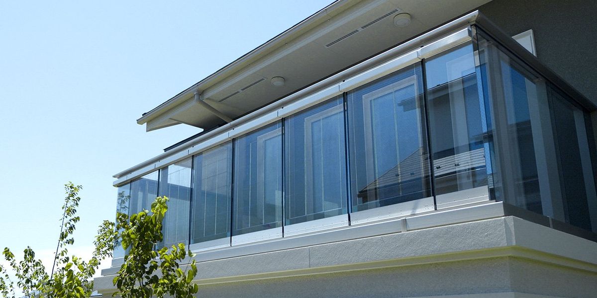
This past August, Panasonic Holdings began testing and demonstrating a prototype version of its perovskite photovoltaic material. The prototype is in the form of semi-transparent glass balustrade panels on the balcony of a model house just south of Tokyo. The panels, each measuring nearly a meter in height and nearly 4 meters in width, are just one of the ways Panasonic intends to enter the building-integrated photovoltaics (BIPV) business.
Sandwiching the perovskite between glass means that it can serve as a building’s actual facades and walls while also generating electricity for on-site use or export to the grid, says Yukihiro Kaneko, general manager of Panasonic’s Applied Materials and Technology Center. He adds that Panasonic can change the material’s level of transparency during the fabrication process, according to a customer’s requirements, which can make it suitable for use as windows.
“Regarding perovskite transparency, what is making the difference is the value of the bandgap,” says Stefaan De Wolf, an engineering professor at King Abdullah University of Science and Technology (KAUST), in Saudi Arabia. “For silicon of a typical thickness (100 to 150 micrometers), it will absorb all available visible photons at 1.2 electron-volts. For perovskite, the bandgap is usually at least 1.5 eV, allowing transmission of the red part of the spectrum. Moreover, perovskite can be printed in patterns, allowing it to act as a neutral-density filter [for color management].”
Panasonic says it can change the degree of transparency in its perovskite to meet customer needs.Panasonic Holdings
But there’s a downside, given the linear relationship that exists between the transparency rate and the perovskite panel’s conversion efficiency. For example, if 50 percent transparency is required in a panel that has an energy-conversion efficiency of 20 percent, the conversion energy efficiency would actually decrease to 10 percent.
The term perovskite refers to a family of compounds, and when used in solar cells, the materials are called perovskite because of their structural similarity to a mineral called perovskite discovered in Russia in 1839. Panasonic has developed its own version of the material with Japan’s New Energy and Industrial Technology Development Organization (NEDO). In 2020, Panasonic achieved a record 17.9 percent conversion efficiency for a large-size perovskite panel.
While silicon is commonly used for solar panels today, perovskite has several advantages, including simpler fabrication methods, lower production costs, flexible design capability, the potential for higher energy conversion efficiencies, and no need for rare earth metals. But it also has some drawbacks, notably that the material will break down when exposed to heat, moisture, or snow—in other words, the very conditions that Panasonic’s BIPV products will constantly face.
To counter this, Panasonic uses two approaches to protect its BIPV devices from the…
Read full article: Perovskite Solar Cells Double as Windows and Walls

The post “Perovskite Solar Cells Double as Windows and Walls” by John Boyd was published on 11/10/2023 by spectrum.ieee.org


